Case Studies
Semiconductor Processing and ceramic machining using MicroBlasting
Why use MicroBlasting for Semiconductor Processing?
MicroBlasting is the ideal method for cutting slots, holes, and apertures in thin, fragile substrates.
- It is a shockless system that does not generate heat into the wafer, preventing crack formation and propagation.
- The cutting effectiveness of the abrasive stream does not change over time – it does not get dull, unlike mechanical tools.
- It’s also easier to clean – the abrasives for this application are environmentally friendly non-toxic minerals.
- Being a dry process, Microbasting avoids the filtration and disposal of water jet technology.
- Our nozzles provide a tight blast stream allowing for thin cuts and small features, and precise control of the blast.
Want to see it for yourself? Watch the clip below:
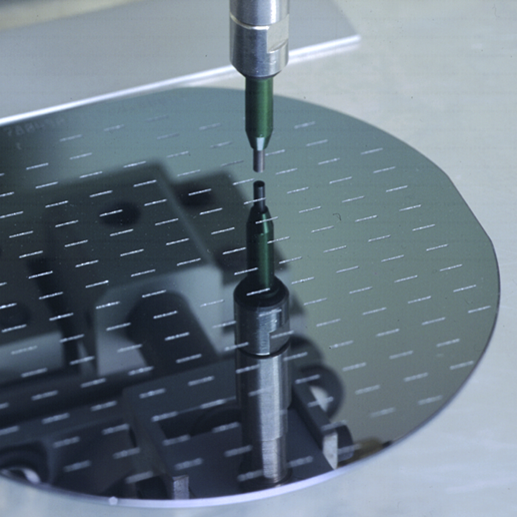
Semicondustor Processing
When you can’t mill a surface
MicroBlasting is the preferred method for thinning parts because, unlike a mill, blasting a part erodes the entire top layer away instead of chopping the top off complex geometries.
Watch the video below for an illustration of how this works:
Thinning silicon dies for semiconductors
One of our customers wanted to thin a silicon die while keeping the part contours the same. More specifically, this part required the removal of over 700 microns of silicon while preserving the curved profile of the part. They also needed to leave a 50 µ layer of protection over the transistors and electronics.
To process this die, we programmed the Advanced Lathe to rotate the part and adjust and adjust the speed of the nozzle as it traversed the die so that it was slower at the edges and faster in the center. This ensured that 700 microns of silicon was removed uniformly from the die
As an example, think of a record player. The needle moves on a longer path at the edges than when it is near the center. The speed of the record with relation to the needle is much faster at the outer edge of the record compared with the inner ring. In our applications we compensate for this by allowing the nozzle to dwell over the outside of the part longer than the inside. The final result is that every location outside the die is processed with the same quantity of abrasive.
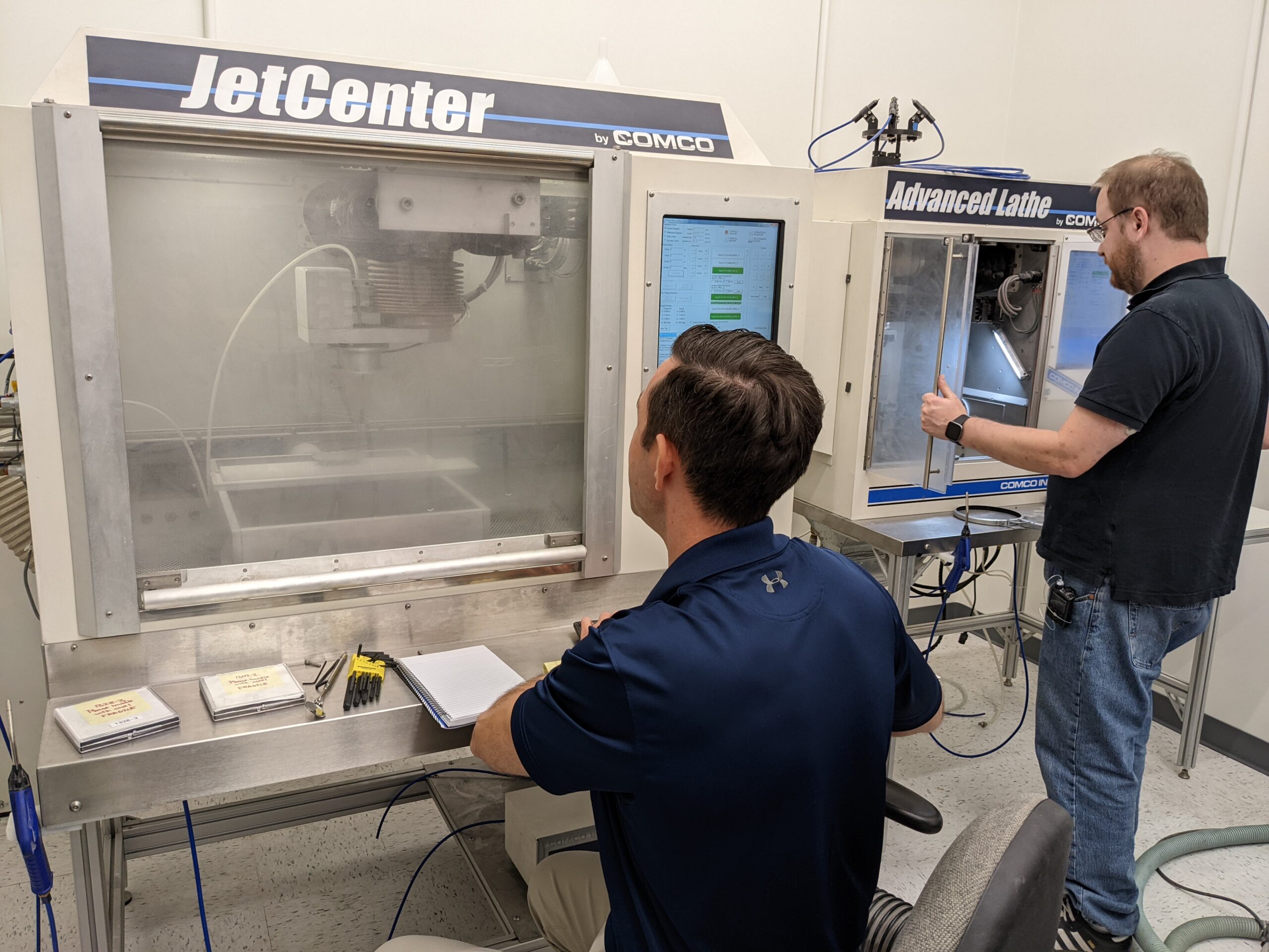
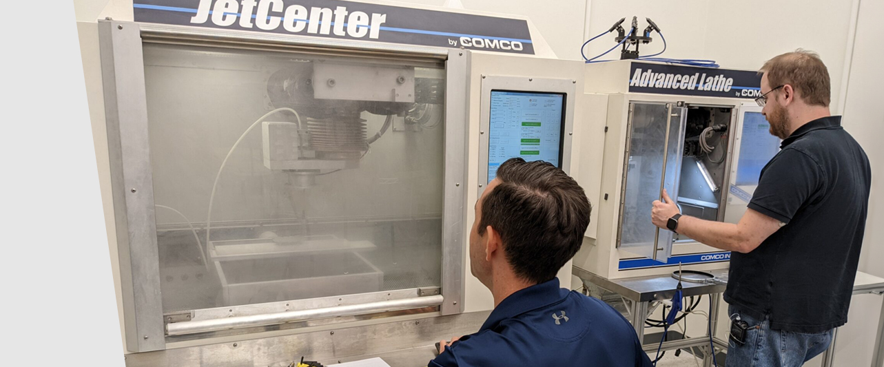
We used our Advanced Lathe to process this part
Nozzle: 0.046″ (MB2520-46)
Distance from Part: 1.625″
Abrasive: 17.5µ aluminum oxide
Blast Pressure: 40 PSI

Microfluidics: Machining without a mask
Inkjet printer cartridges are a perfect example of a silicon wafer part that’s best cut with MicroBlasting. The via, or hole, that connects the ink reservoir to the individual nozzles is carved into the same silicon wafer that manages the signal. This via must be milled into the middle of each silicon wafer segment and its shape is critical to flow of ink to each nozzle.
MicroBlasting cuts an organic shape in a silicon wafer, improving the fluid dynamics of the ink flow. Even better, a micro-abrasive stream can mill without generating heat or vibration, limiting the formation of micro-cracks.
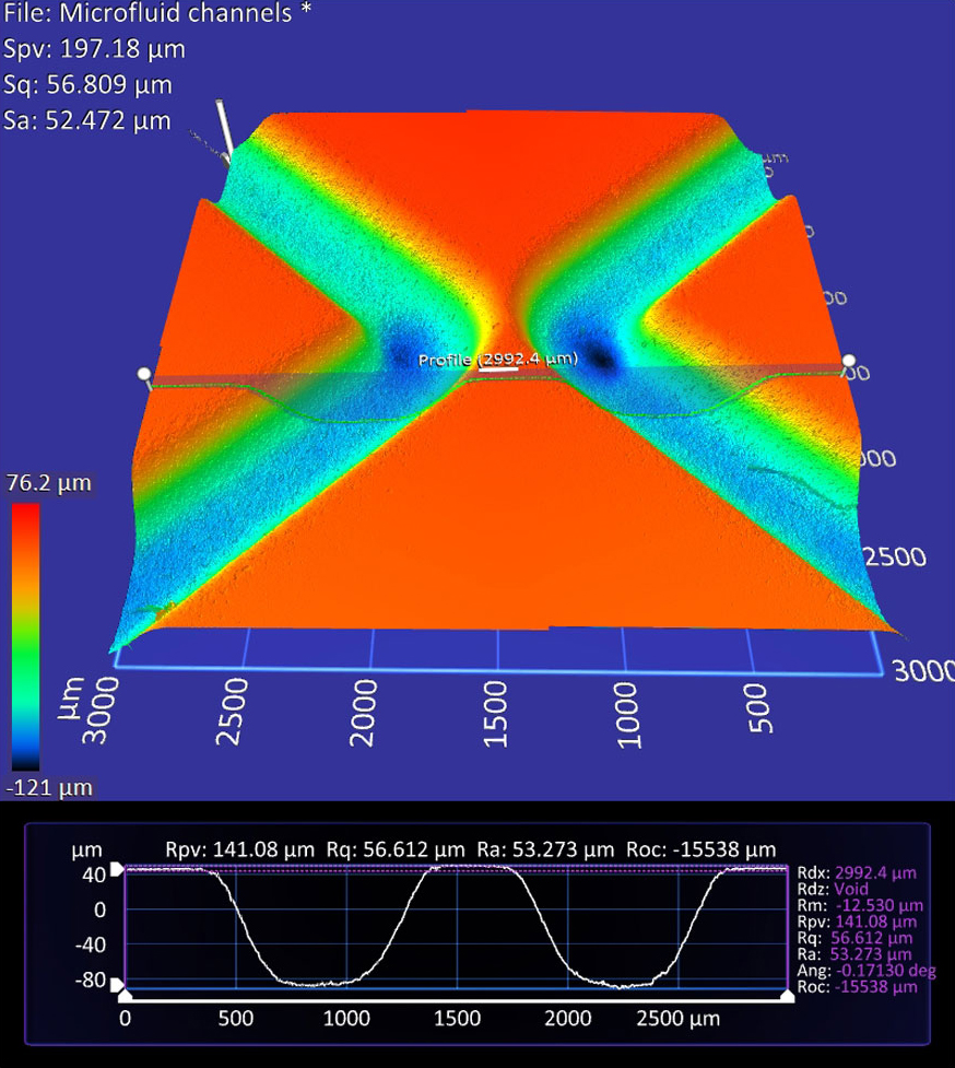
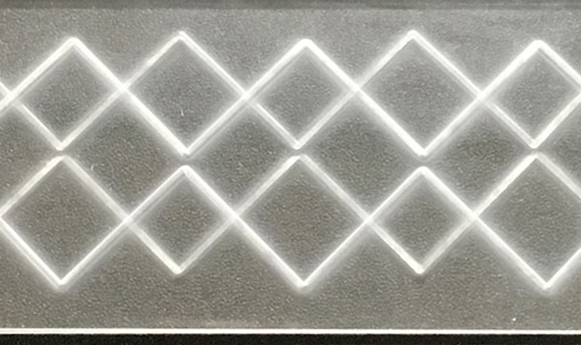
Likewise, blood mixers have a similar layout. In the application pictured below, our customer used MicroBlasting to cut two microchannels into the top and bottom glass slides on a blood mixer. This particular design allows fluids to properly mix at channel intersections.
The channels were cut with a 0.030″ Comco Hi/Performance (MB2520-30 nozzle) blasting 17.5 aluminum oxide at 50 PSI. Unlike most applications, the nozzle distance was close (0.05″) to the target. Holding the nozzle close to the part cuts a trough with relatively steep sides without using a mask.
MEMS
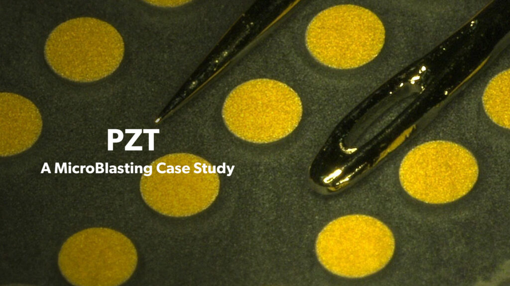
MicroBlasting is also a great method of etching small features into piezoelectric ceramic material (PZT). In fact, researchers at the University of Maryland recently determined that etching using MicroBlasting is mass-producible, commercially viable, fast, and inexpensive. The following paper, published in the Journal of Micromechanics and Microengineering, dives into the methodology behind the process.
The researchers detail why MicroBlasting is an excellent tool for creating microelectrical systems (MEMS) from bulk PZT that has been patterned using a dry-film photoresist mask. They also show how abrasive type, blast pressure, and nozzle-to-part distance can be manipulated to control etching rates and create features as small as 25 microns—all without undercutting the mask.
The team used MicroBlasting to create two different cantilever micro-actuators. They concluded that using our technology on dry-film patterned PZT greatly simplified fabricating devices out of bulk PZT compared to other existing techniques. The entire fabrication process for each device took less than an hour, allowing for the rapid development of a range of micromechanical devices to be built out of bulk PZT.
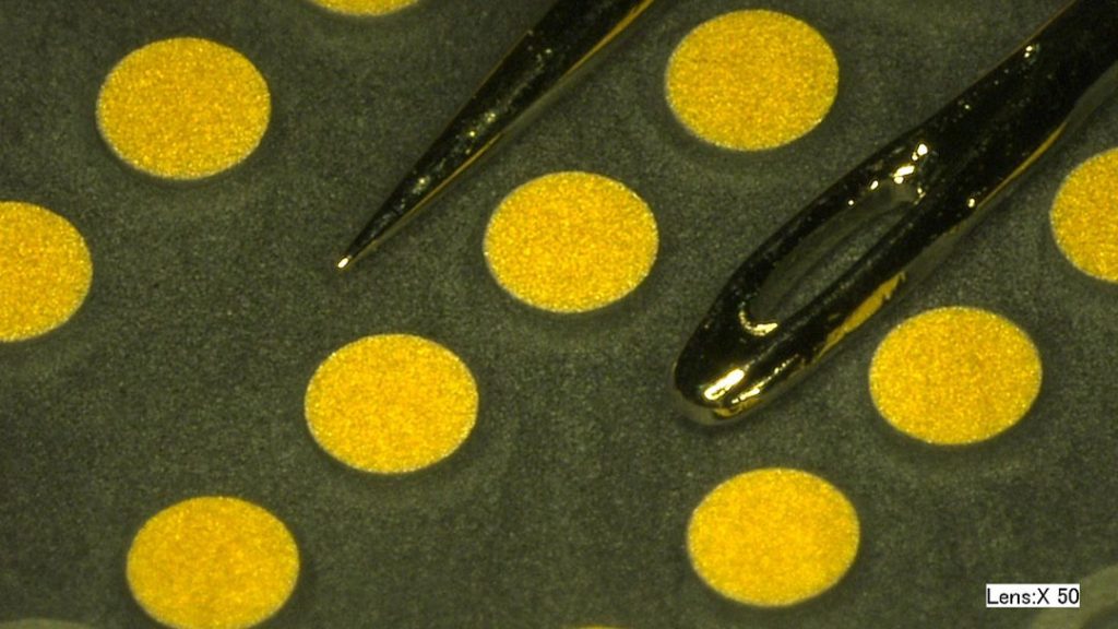
Wafer Coring, Slotting and Beveling
MicroBlasting is a great method of coring and slotting brittle wafers, especially if a beveled edge to the slot is needed. This process naturally creates a sloped wall on the cut edge that is difficult to machine with other methods.
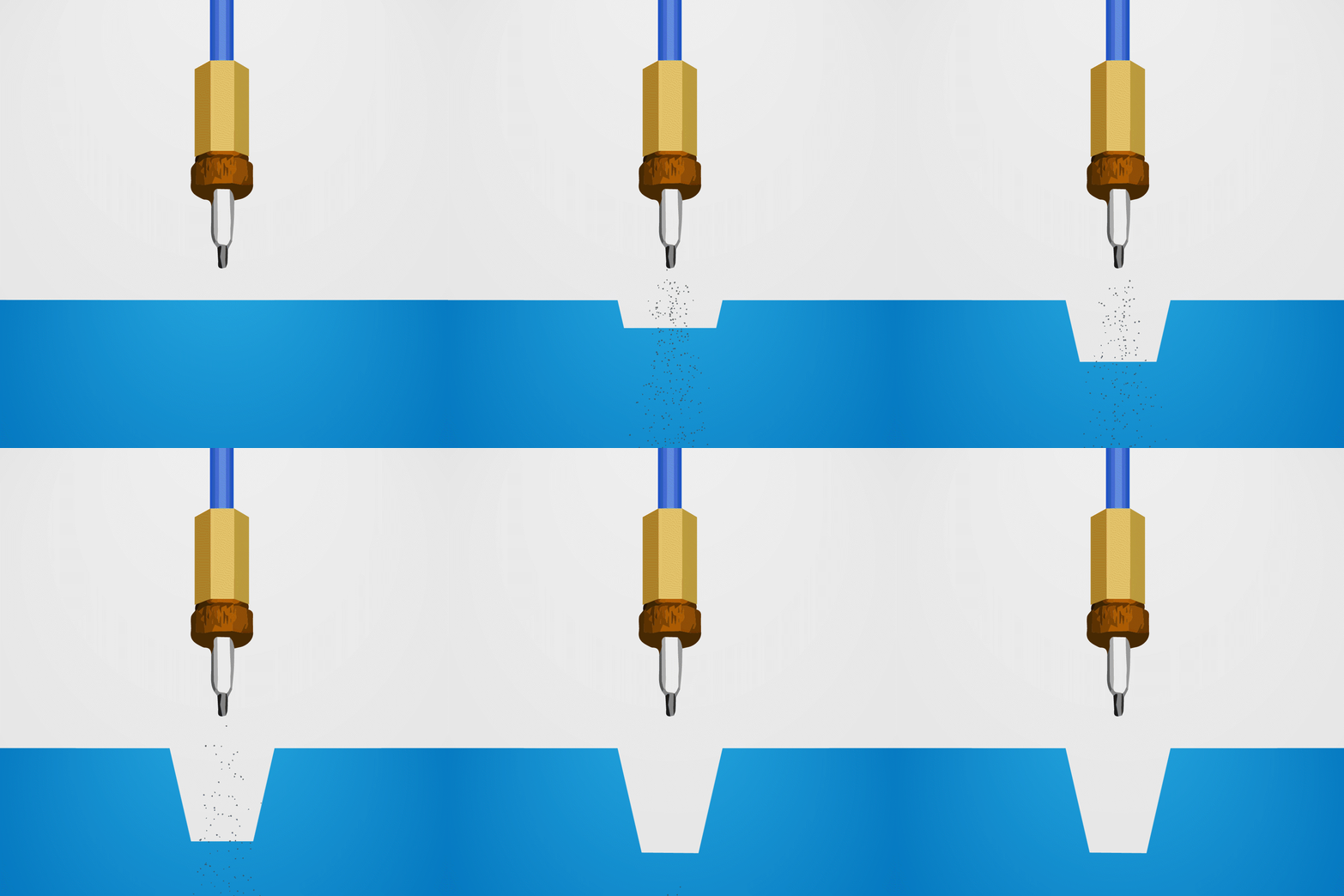
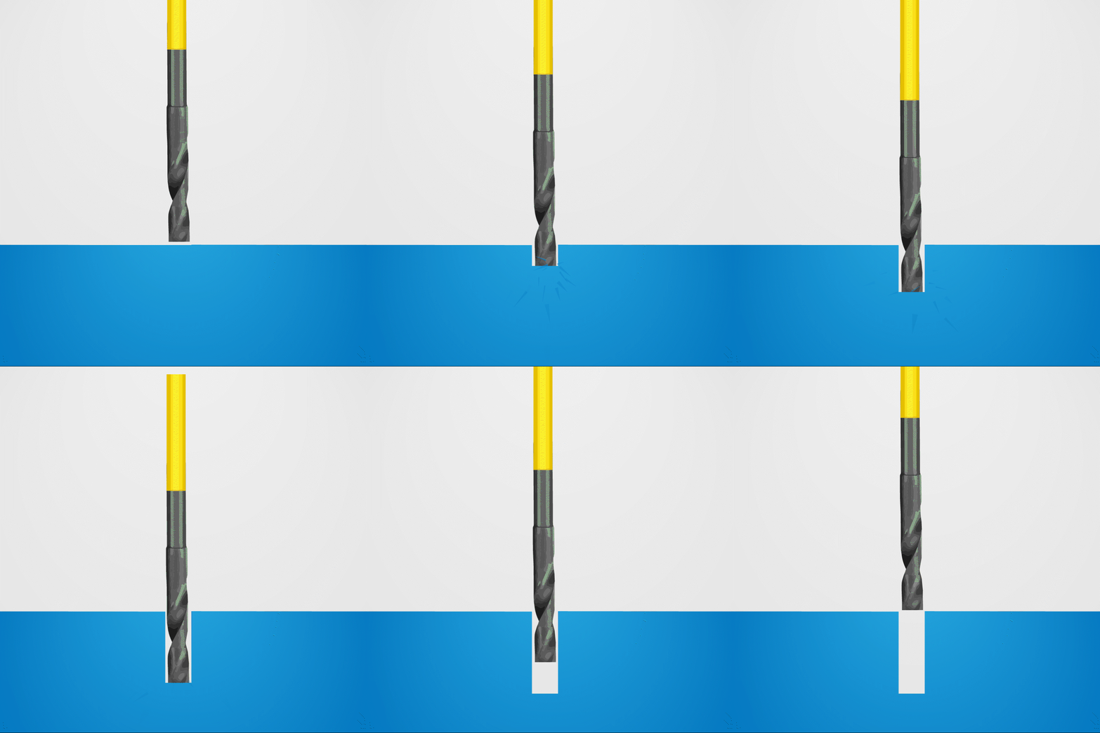
Similarly, our process is also great for coring to create both circular and rectangular wafers. Since MicroBlasting is shockless and heatless, there’s less chance of micro-fractures forming in the part while a piece is cut from the center while the die is cut from the center of a larger wafer.
Improve Semiconductor Processing with Automation
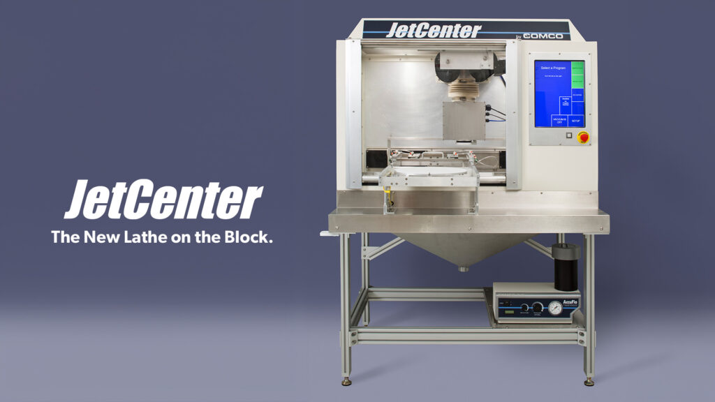
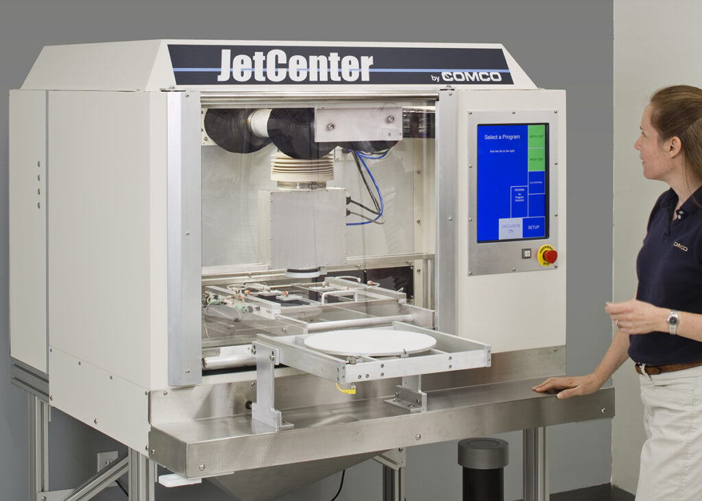
If you you have a large volume of parts to process, or need identical specifications for every part, automation might be right for you. With our automated systems, you can reliably and repeatedly cut complex shapes while processing semiconductors. Additionally, our TwistWrist technology allows an angled nozzle to be rotated and positioned for angled/beveled cuts, always preserving the angle of the nozzle with respect to the edge regardless of the direction of the cut.
Applications Lab
Let our experts help find the right solution for your part. We know no two applications are the same. Our Technical Specialists manage sample-part testing and processing from start-to-finish. They actively collaborate with our Sales and Engineering Teams while remaining completely accessible to you throughout the process.
